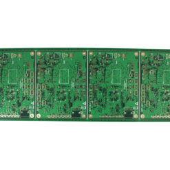
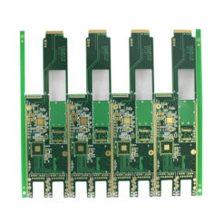
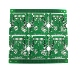
High density interconnects (HDI) PCB, represent one of the fastest-growing technologies in PCBs. Because of its higher circuitry density than traditional circuit boards, the HDI PCB design is able to incorporate smaller vias and capture pads, and higher connection pad densities.
1. Can reduce the cost of PCB: When the density of the PCB increases by more than eight layers, HDI PCB is used to make 2, 2, and the cost will be lower than the traditional complicated lamination process.
3. Increase circuit density: the interconnection of traditional circuit boards and parts
4. Conducive to the use of advanced construction technology
5, with better electrical performance and signal accuracy
6, better reliability
7, can improve thermal properties
8. Can improve radio frequency interference / electromagnetic wave interference / electrostatic discharge (RFI / EMI / ESD)
9. Increase design efficiency


